Don't Route Over Ground Plane Splits — Part 1: Emissions
Everyone says not to route traces over splits in ground planes. Two custom microstrip test boards, a TEM cell, and a spectrum analyzer show you exactly what happens when you do.
The rule everyone quotes
"Never route a signal trace over a split in the ground plane." Every PCB design guide says it. Every EMC consultant repeats it. But I haven't seen many people actually measure it.
There are countless resources online that explain why this is a bad idea (return current paths, loop area, slot antennas), and they do it far better than I could. The YouTuber Baltic Lab did a similar experiment using near-field probes and also demonstrates crosstalk effects on his demo boards. Worth watching. I'm not going to cover the theory here. The plan is to measure the boards first in the TEM cell for quick, repeatable pre-compliance data, then take the same boards to an accredited EMC lab and measure them in a proper anechoic chamber. That gives us bench-level comparative TEM-cell data and, later, formal chamber data on the exact same DUT. They are not the same measurement, but together they should show how well the bench setup predicts the bigger test. Measurement results will follow once the lab work is complete.
The test boards
Two four-layer microstrip boards, identical in every way except one: the second board has a deliberate split across the ground plane, directly under the signal trace.
Both boards are simple: a 50 Ω microstrip trace on the top layer, running between two edge-launch SMA connectors, with the main reference plane on layer 2 directly below the trace. The trace is impedance-controlled, width calculated for 50 Ω on the chosen stackup. Four mounting holes in the corners allow the boards to be bolted down during testing. One SMA port is terminated with a 50 Ω load to absorb reflections, so the unused end is properly matched.
Board A — intact ground plane (reference)
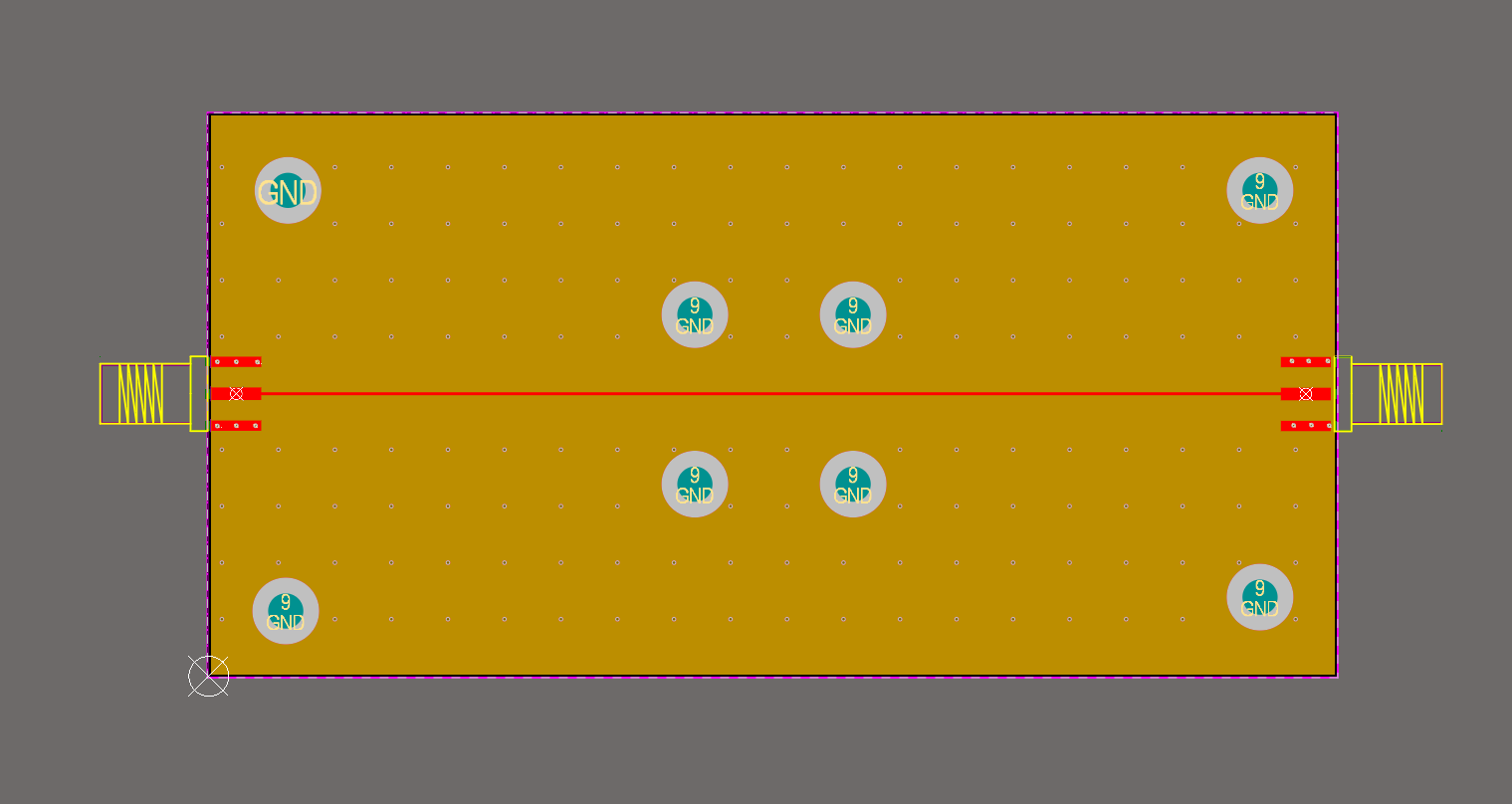
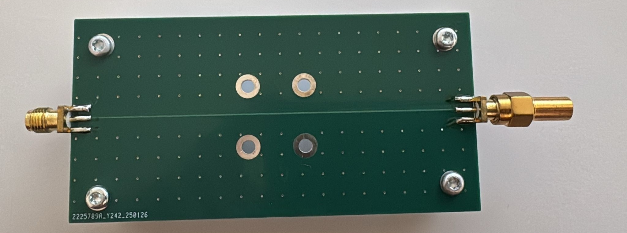
The reference board. Continuous reference copper under the trace, with no interruption in the return path. The return current flows directly underneath the signal trace, which is the lowest-inductance path. The fabricated board also has extra ground vias around the SMA launches to keep the connector transition well referenced.
Board B — split ground plane
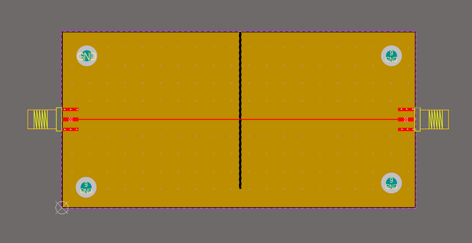
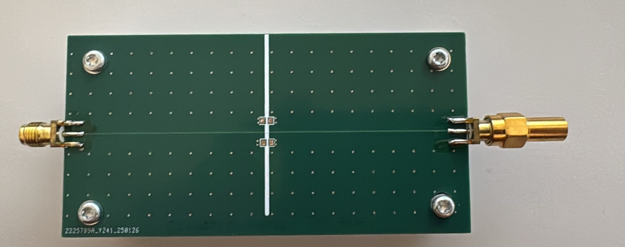
Same board, same trace, same connectors — but with a slot cut through the bottom ground plane, running perpendicular to the signal trace. The slot extends almost the full width of the board. The trace crosses directly over the gap. On the fabricated board, the split is clearly visible as a white line across the board. Two 0603 pads bridge the gap at the trace crossing point — these are for stitching capacitors. For the baseline measurement, these pads are left unpopulated. Later, capacitors will be soldered in to test whether stitching caps can recover the damage.
Design details
- Stackup: 4-layer, FR4
- Trace type: Microstrip (top layer trace, ground plane on layer 2)
- Impedance target: 50 Ω
- Connectors: Edge-launch SMA (both ends)
- Termination: 50 Ω load on one SMA port to absorb reflections
- Board dimensions: Identical for both variants
Equipment
The measurement will use radiated emissions in a TEM cell and later an anechoic chamber. Detailed specs for each instrument are linked below.
- Siglent SSA3032X-R spectrum analyzer — the receiver (9 kHz to 3.2 GHz)
- Tekbox TBTC3 TEM cell — converts radiated emissions from the board into a conducted signal for the analyzer
- Tekbox TBST-120/60/60/2-B shielded tent — keeps ambient RF out of the measurement
- Tekbox TBCG4 comb generator — broadband signal source with harmonics every 10 MHz, fed into one SMA port of the test board
- Leo Bodnar LBE-1320 fast pulse generator — 30 ps rise time, a second signal source to confirm results with more realistic edges
Verifying the comb generator
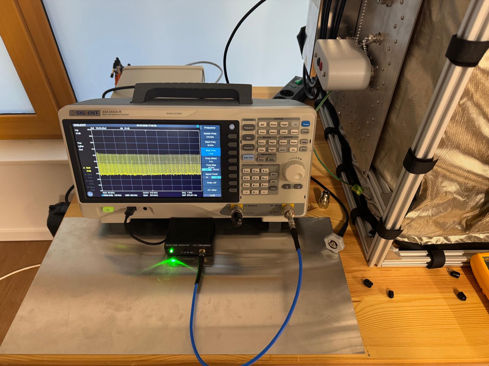
Before measuring the boards, a sanity check: the TBCG4 comb generator connected directly to the spectrum analyzer through a 10 dB attenuator to verify the signal source is working as expected.
Frequency domain
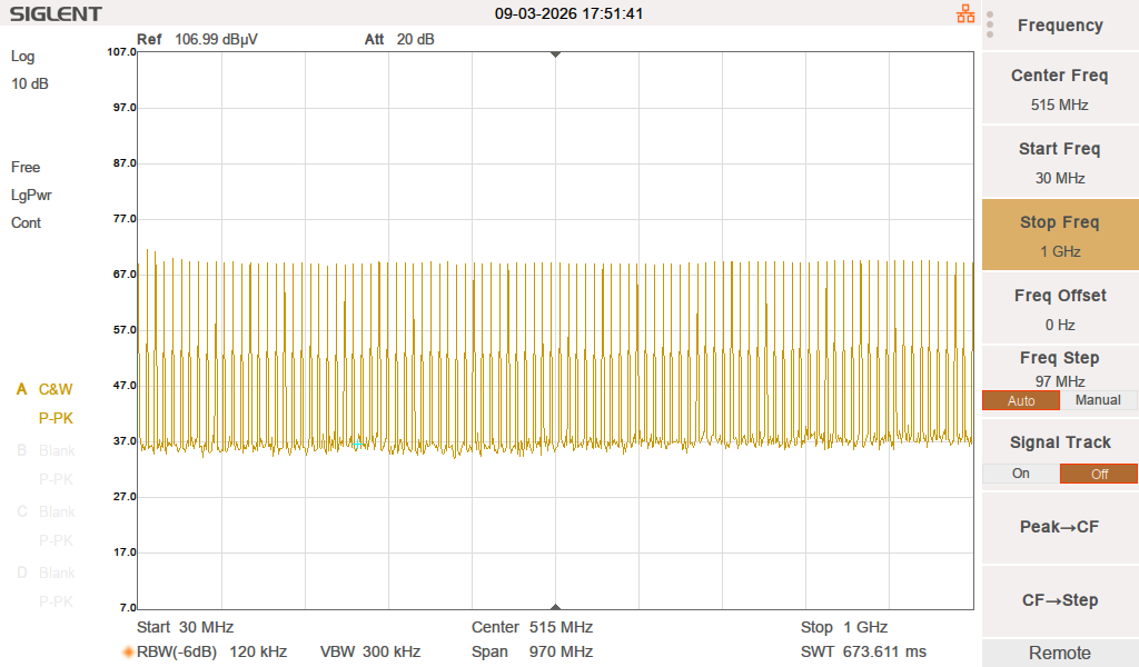
Spectrum analyzer settings: 30 MHz to 1 GHz span, RBW 120 kHz, VBW 300 kHz, positive peak detector, 20 dB input attenuation, reference level 107 dBuV, 10 dB/div. The comb harmonics are clearly visible every 10 MHz, flat across the band at roughly 65 dBuV — the TBCG4 lives up to its spec.
Verifying the Leo Bodnar pulser
Same setup, same SA settings — but with the LBE-1320 pulse generator instead of the comb generator.
Frequency domain
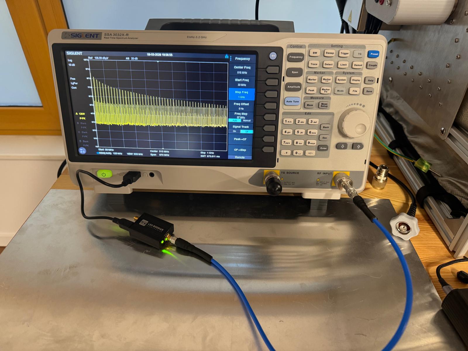
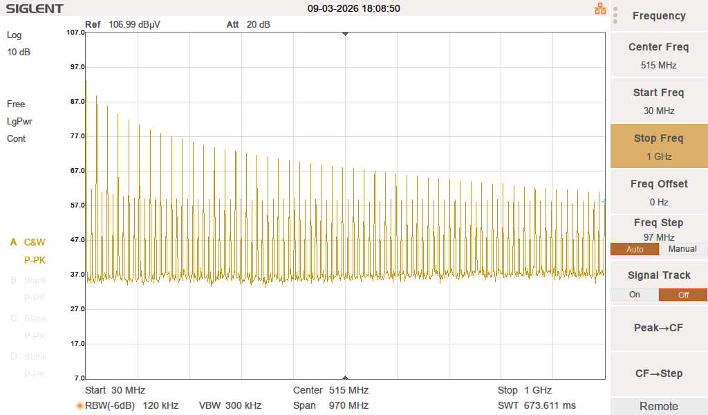
The spectrum looks very different from the comb generator. Instead of flat, evenly spaced harmonics, the pulser produces a broad spectral envelope that is strongest at lower frequencies and rolls off toward higher frequencies. That makes it a more useful broadband stimulus for this comparison, even if it is still only a simplified stand-in for real digital edge spectra.
Measurement setup
The TEM cell sits inside the shielded tent. The test board is placed on the TEM cell septum, comb generator connected to one SMA port, 50 Ω termination on the other. The spectrum analyzer is connected to the TEM cell output through the tent's N-type feedthrough.
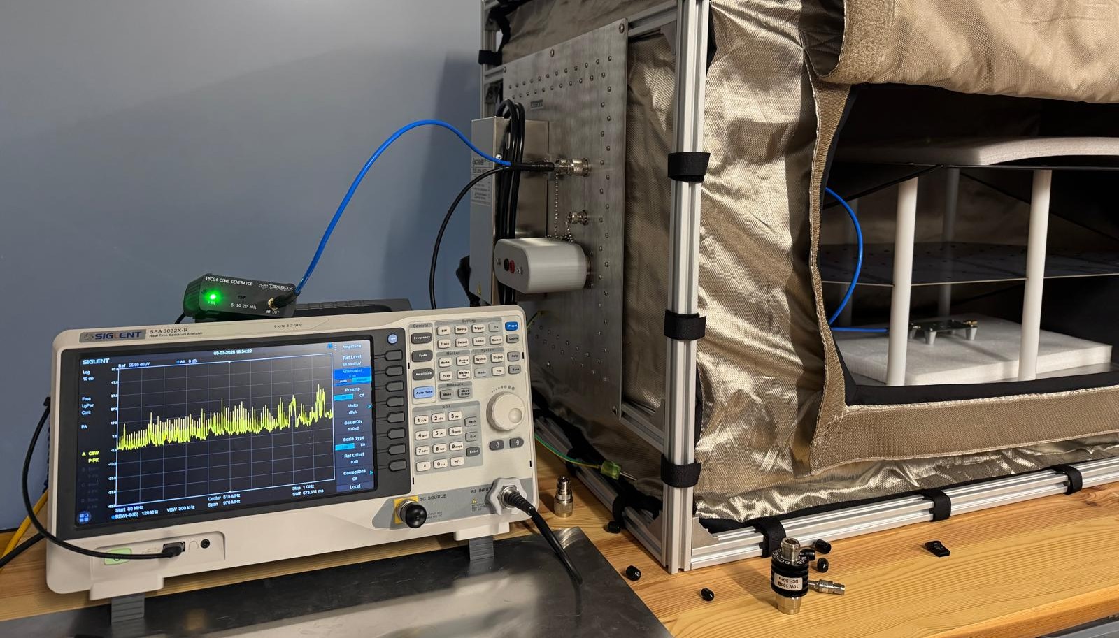
The photo shows the setup with the tent open. The actual spectra were captured with the tent closed to block ambient RF.
Important note on DUT placement: The board orientation inside the TEM cell matters — rotating the board 90° or 180° on the septum can change the coupling and the measured spectrum. All measurements in this article were taken with the board in a single, fixed orientation. In a real pre-compliance scenario, you should test multiple orientations and take the worst case.
SA settings for all TEM cell measurements: 30 MHz to 1 GHz span, RBW 120 kHz, VBW 300 kHz, positive peak detector, reference level 57 dBuV, 0 dB input attenuation, preamp ON, 10 dB/div. The preamp and zero attenuation are needed because the signal through the TEM cell is much weaker than a direct connection.
Results
Each board was measured with both signal sources. The three raw spectrum captures were taken at different SA settings (the split board was so much hotter that the reference level and attenuator had to be raised just to fit the trace on screen), so comparing screenshots side by side is misleading. Instead, the plots below overlay all three boards on the same axes. The solid lines are smoothed envelopes that follow the peak tops of each trace. You can toggle the raw spectrum data on if you want to see the actual peaks. Hover for readout values at any frequency.
Comb generator
Leo Bodnar pulser
Both sources tell the same story. The split board (red) is dramatically worse across the entire band — on average about 17 dB worse, with the worst individual frequencies exceeding 40 dB. That is not a marginal difference; it is the difference between passing and catastrophically failing an EMC test. Emissions rise with frequency as the slot becomes a more efficient radiator.
Stitching caps (blue) recover most of the damage at lower frequencies — about 16 dB on average — but lose effectiveness above ~600 MHz where parasitic inductance dominates. At some individual peaks above 800 MHz the caps board is still up to 27 dB worse than the intact board. They help, but they are a compromise, not a fix.
The fact that both sources — discrete harmonics and continuous spectrum — produce nearly identical deltas confirms the result is geometry-driven, not source-dependent.
Why this happens
Any reference plane discontinuity — a split, a gap, a slot, a cutout — forces the return current to detour around it. The return path gets longer, the loop area increases, and the board radiates more. The same applies whether it is a deliberate split or an accidental gap from a connector keepout or a routing channel.
The discontinuity itself can also resonate as a slot antenna, producing narrow emission peaks at frequencies where the slot length approaches a half wavelength. On slow signals the effect may be small, but once the edge rates get fast enough the extra radiation shows up clearly.
Practical takeaways
Keep high-speed traces over a continuous reference plane, and do not cross splits, cutouts, or notches unless you have no other option.
Watch for accidental gaps too. In practice, they often come from copper cutouts, connector keepouts, or routing that breaks the plane into islands.
If a split is unavoidable, force the crossing through one controlled location and verify it with measurement. Stitching capacitors can help in some cases, but they are a compromise, not a substitute for a solid plane.