Don't Route Over Ground Plane Splits — Part 3: The Loop and Its Area
A DIY near-field EMC scanner built from a Snapmaker A350 and a Siglent spectrum analyzer reveals the emission pattern of ground plane splits — frequency by frequency, overlaid on the actual board photos.
From numbers to pictures
In Part 1 and Part 2, I compared the boards using a TEM-cell bench setup. That gives a useful comparative measurement, but it does not tell you where on the board the activity comes from.
A near-field scanner does. It moves a small probe across the board surface on a grid, capturing the spectrum at each point. The result is a spatial map of the electromagnetic emissions at any frequency, overlaid directly on the board photo.
Parts 1 and 2 gave us numbers. This one gives us pictures.
The poor man's scanner
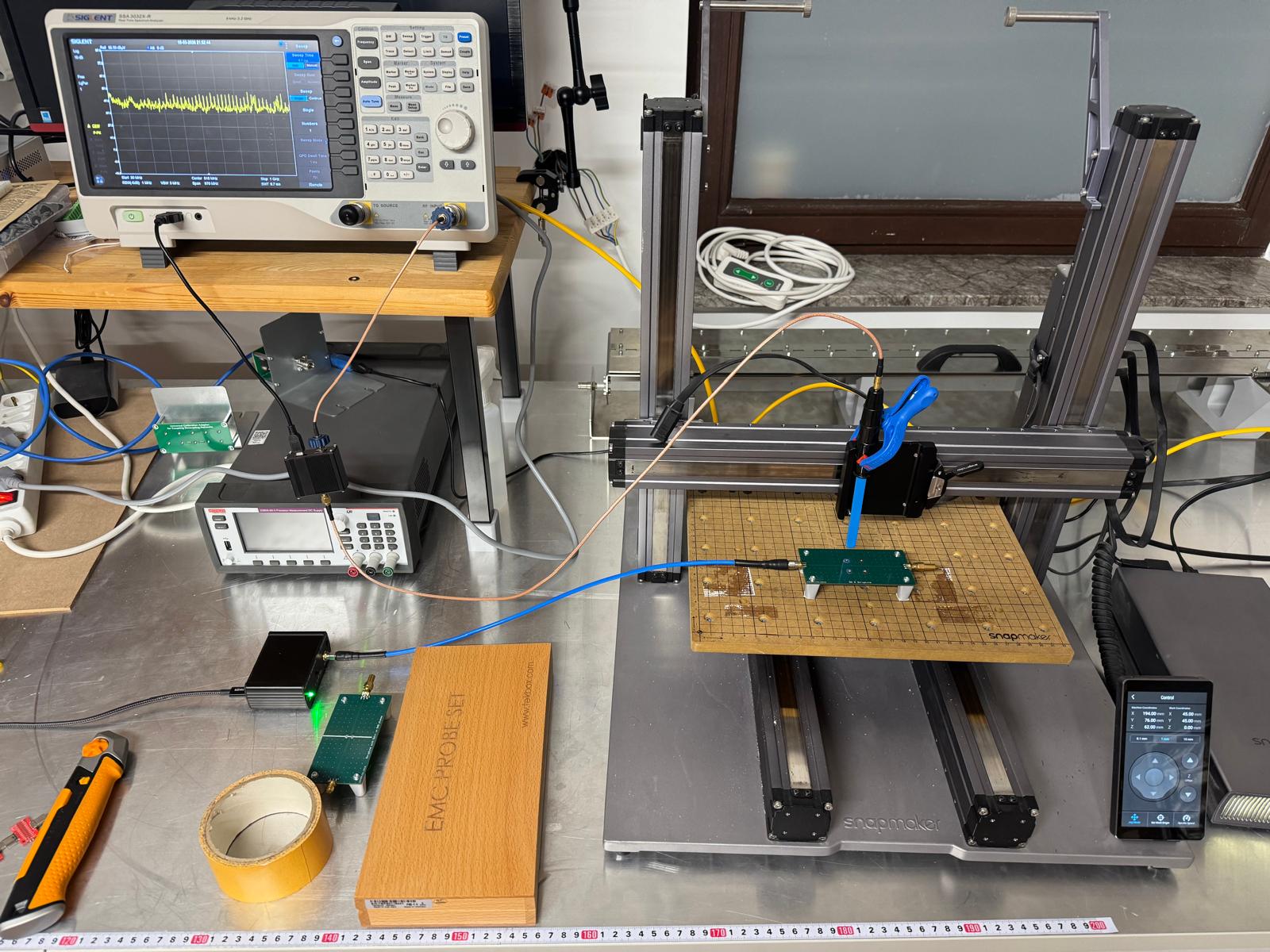
The scanner is built entirely from equipment already in the lab:
- Motion platform: Snapmaker A350 — a 3D printer repurposed as an XY stage. The CNC toolhead is replaced with a clamp holding the near-field probe. Controlled via USB serial with standard G-code.
- Spectrum analyzer: Siglent SSA3032X-R — configured for triggered single sweeps (30 MHz to 1 GHz, RBW 1 MHz). Controlled via SCPI over TCP.
- Probe: Tekbox TBPS01 near-field H-probe.
- Preamp: Tekbox TBWA2 — 40 dB wideband amplifier, used for the intact board scan to boost the low emission levels.
- Signal source: Tekbox TBCG4 comb generator set to 10 MHz fundamental — same source used in Parts 1 and 2, fed into the board's SMA input. The heatmap slider only includes harmonics of 10 MHz.
A Python script orchestrates the whole process: move to a grid point, wait for the probe to settle, trigger a sweep, read the full 751-point trace, save it as CSV, move to the next point. The scan follows a serpentine pattern to minimize travel time.
The scan area covers the full board: 98 x 49 mm at 2 mm resolution — 1,250 points per board per probe orientation. Each board was scanned twice — once with the H-probe in the X orientation and once in Y — and the heatmaps show the worst case at each point, combining both components into a single map. Each scan takes about 5 minutes.
The boards
Same three boards from Parts 1 and 2:
- Intact ground plane — solid copper pour under the signal trace. The reference.
- Split ground plane — a slot cuts across the ground plane directly under the trace, forcing the return current to detour around the split.
- Split with stitching capacitors — two 100 nF 0603 capacitors (CC0603KRX7R9BB104) bridging the slot.
Results
Drag the slider to see the near-field emission pattern at each frequency. The heatmap is overlaid directly on the board photo — brighter means stronger emission. All three boards are on the same color scale, so the maps are directly comparable.
Intact ground plane
The intact board shows a clean emission pattern: the signal trace lights up as a narrow band across the middle. The radiation is concentrated along the trace and drops off to either side. The return current flows directly beneath the trace in the ground plane, keeping the loop area small.
Split ground plane
Very different picture on the split board. The slot forces the return current to find an alternative path — around the edges of the split. This creates a large current loop that acts as an antenna. At higher frequencies, the entire board lights up. The radiation pattern is no longer a tight line — it's a broad dome. This is the loop, and you're looking at its area.
Split with stitching capacitors
The stitching capacitors provide a partial bridge across the slot. At frequencies where the caps present low impedance, the return current can cross the gap — reducing the loop area and the resulting emissions. The pattern sits between the intact and split boards: better than the open split, but not as clean as a solid ground plane.
What the scanner shows
The TEM cell measurements in Parts 1 and 2 gave us numbers: the split board radiates more, the caps help somewhat. The near-field scan shows why and where:
- Intact board: emission follows the trace. Small loop, low radiation.
- Split board: emission spreads across the entire board. The return current loop has become a large antenna.
- Stitching caps: the pattern pulls back toward the trace, but the improvement is frequency-dependent.
The title of this series says "Don't route over ground plane splits." These heatmaps show you exactly what happens when you do.